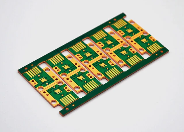
HEAVY COPPER AND EXTREME COPPER IN PCB DESIGN
Standard PCBs are manufactured with copper traces/planes made up of copper weights ranging from 0.5oz to 3oz copper. A heavy copper circuit ranges from 4oz to 20oz. An extreme copper circuit can be 20oz up to 200 oz.
Some benefits of thick copper PCBs:
- Increased thermal endurance (also, heavy copper plated vias carry higher current through the board and help to transfer heat to an external heatsink)
- Increased current carrying capacity
- Increased mechanical strength for plated through holes
- On-board heatsinks directly plated onto the board surface using up to 120-oz copper planes
- On-board high-power-density for planar transformers
Design features:
- 1-30 layers is possible
- Extreme copper is possible on outer layers. Up to 12oz on inner layers
- Standard Tg 140°C up to Tg 170°C
- Min. Track/Spacing
- External layers
- 4oz – 10mil/13mil
- 5oz – 12mil/15mil
- 6oz Cu 15mil/15mi
- Internal layers
- 4oz – 8mil/8mil
- 5oz – 10mil/10mil
- 6oz – 12mil/12mil
- External layers
- Min. Hole size – 0.15 ~ 0.3mm
- Board thickness – 0.6mm – 6mm
- Standard surface finishes
- Standard soldermask and silkscreen options
- Build time 5-15 days